Product Detail
SYN8205W3
synapsechip.comOur Products
Specifications
- Configuration
- N+N
- VDS_Max
- 20 V
- VGS(th)_Typ
- 0.7 V
- Die Size (μm×μm)
- 961*602(不含划片槽)
- Gross Die (12" wafer)
- 97000
- Wafer Thickness (μm)
- 150
- RDS(ON)_Typ @VGS=4.5V
- 16.5 mΩ
- RDS(ON)_Max @VGS=4.5V
- 24 mΩ
- RDS(ON)_Typ @VGS=2.5V
- 20.5 mΩ
- RDS(ON)_Max @VGS=2.5V
- 35 mΩ
- Tj
- -55~+150 °C
Not sure how to choose? Read the MOSFET Wafer & Bare Die Selection Guide →
Online Datasheet
Full text of the synapsechip.com datasheet; refer to the latest revision for updates.

SYN8205W3
20V Dual N-Channel Enhancement Mode MOSFET
WAFER DATASHEET
Features
- V(BR)DSS = 20 V, ID = 4.2 A
- RDS(ON) < 24 mΩ (max.) @ VGS = 4.5 V
- RDS(ON) < 35 mΩ (max.) @ VGS = 2.5 V
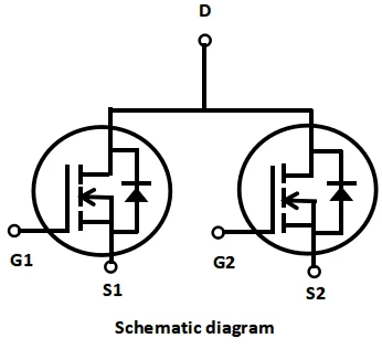
- Dual N-Channel, Common-Drain Configuration
- High Power and Current Handling Capacity
- Lead-Free Product
- For Surface Mount Packages
Applications
- PWM Application
- Load Switch
- Power Management
Chip Information
| Parameter | Value |
|---|---|
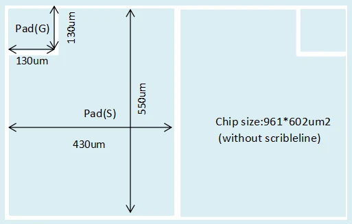
| Die Size (without scribe line) | 961 μm × 602 μm (dual N) |
| Gate Pad Size | 130 μm × 130 μm × 2 |
| Source Pad Size | 430 μm × 550 μm × 2 |
| Scribe Line Size | 60 μm |
| Wafer Thickness | 150 μm |
| Wafer Diameter | 300 mm, with (100) notch |
| Front Metal Composition & Thickness | AlCu, 4 μm |
| Back Metal Composition & Thickness | Ti-Ni-Ag, 1kÅ-2kÅ-10kÅ |
| Gross Die (approximately) | 97,000 |
Ordering Information
| Orderable Part Number | Product Form | Wafer Diameter | Shipping Option |
|---|---|---|---|
| SYN8205W3 | Un-sawn Wafer | 300 mm | Un-sawn wafer (standard) |
Maximum Ratings
(@ TA = 25 °C, unless otherwise specified.)
| Characteristic | Symbol | Value | Units |
|---|---|---|---|
| Drain – Source Voltage | VDS | 20 | V |
| Continuous Drain Current | ID | 4.2 | A |
| Operating and Storage Temperature | TJ, TSTG | −55 ~ +150 | °C |
Electrical Characteristics
(@ TA = 25 °C, unless otherwise specified.)
Off Characteristics
| Parameter | Symbol | Test Conditions | Min. | Typ. | Max. | Units |
|---|---|---|---|---|---|---|
| Drain–Source Breakdown Voltage | V(BR)DSS | VGS = 0 V, ID = 250 μA | 20 | 22.5 | — | V |
| Zero Gate Voltage Drain Current | IDSS | VDS = 20 V, VGS = 0 V | — | — | 100 | nA |
| Gate–Body Leakage Current | IGSS | VGS = ±12 V, VDS = 0 V | — | — | ±100 | nA |
On Characteristics
| Parameter | Symbol | Test Conditions | Min. | Typ. | Max. | Units |
|---|---|---|---|---|---|---|
| Gate Threshold Voltage | VGS(th) | VGS = VDS, ID = 250 μA | 0.5 | 0.7 | 1.0 | V |
| Static Drain–Source On-Resistance (CP) | RDS(ON) | VGS = 4.5 V, ID = 1 A | — | 16.5 | 24 | mΩ |
| Static Drain–Source On-Resistance (CP) | RDS(ON) | VGS = 2.5 V, ID = 1 A | — | 20.5 | 35 | mΩ |
Shipping, Handling and Storage
| Item | Requirement |
|---|---|
| Shipping | One shipping option is offered as standard: un-sawn wafer. Sampling CP test is performed in order to guarantee minimum yield. |
| Handling | Product must be handled only at ESD safe workstations. Standard ESD precautions and safe work environments are as defined in MIL-HDBK-263. Product must be handled only in a class 10,000 or better-designated clean room environment. |
| Wafer Storage | Proper storage conditions are necessary to prevent product contamination and/or degradation after shipment. Un-sawn wafers and singulated die can be stored for up to 12 months when in the original sealed packaging at room temperature (45% ± 15% RH controlled environment). Un-sawn wafers and singulated die that have been opened can be stored when returned to their containers and placed in a nitrogen purged cabinet, at room temperature (45% ± 15% RH controlled environment). Sawn wafers on a film frame are intended for immediate use and have a limited shelf life. |
Notes
- Electrical characteristics are referenced to the die assembled in a TSSOP-8 package. Bonding wire reference: Gate — Cu 1.65 mil × 2; Source — Cu 1.65 mil × 6 × 2.
- (CP) Parameter verified by sampling chip-probe (wafer sort) test.
- To reduce the risk of contamination or degradation, it is recommended that product not being used in the assembly process be returned to its original container and resealed with a vacuum seal process.
Important Notice
Information in this document is provided in connection with 突触半导体 products and is subject to change without notice. Customers are responsible for verifying that the product is suitable for their application; no license to any intellectual property right is granted by this document.
SYN8205W3 · Rev 1.0 · 2026-08 深圳市突触半导体有限公司 · synapsechip.com Page 2 of 2