
The 2nd Forum on High-Quality Development of Electrical Equipment for New Power Systems took place in Shanghai on 7–8 November 2024. It was guided by the China Machinery Industry Federation, supported by the China Electrical Equipment Industry Association, and hosted by Shanghai Electrical Apparatus Research Institute (Group) Co., Ltd. together with Shanghai Electrical Apparatus Research Institute Technology Co., Ltd.
During the forum, TILVA (Shanghai TILVA Certification Technology Co., Ltd.), the certification brand of the Shanghai Electrical Apparatus Research Institute group, formally presented SineSemi (Shanghai) Semiconductor Co., Ltd. with a product certificate for power semiconductor devices used in PV-storage-charging energy conversion equipment. It is the first certificate issued under this category, and the certified product is a power semiconductor device (MOSFET).
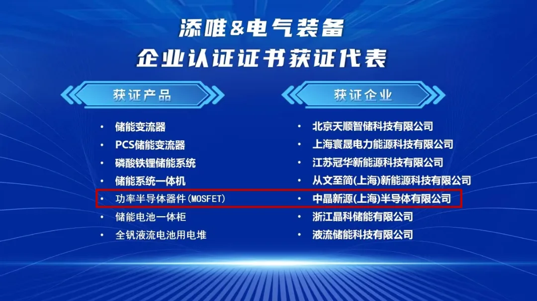
Recipients of TILVA electrical-equipment enterprise certificates; SineSemi's certified product is a power semiconductor device (MOSFET). Image: SineSemi
The certification involved technical evaluation and testing of electrical performance, thermal performance and quality reliability, and found that SineSemi's power devices meet the technical requirements and quality standards that PV-storage-charging energy conversion equipment places on power semiconductors.
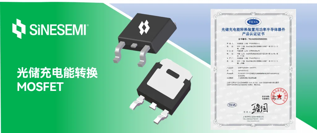
SineSemi MOSFETs for PV-storage-charging energy conversion, with the product certificate issued by TILVA. Image: SineSemi
SineSemi's stated mission is "driving the green new-energy revolution with Chinese chips". For the PV, energy-storage and charging market it fields three product lines — high-voltage superjunction (SJ) MOSFETs, SGT MOSFETs and IGBT modules — built around the following design points:
High-voltage SJ MOSFETs
- Redundant die design for stronger avalanche and short-circuit current capability;
- Optimized body diode for higher dv/dt ruggedness, lower Qrr and smaller voltage spikes;
- Tuned Qg and Crss/Ciss ratio to cut switching loss and improve noise immunity;
- Deep-trench and multi-layer epitaxy processes developed in parallel to cover a range of application requirements.
SGT MOSFETs
- FOM (RDS(ON) × Qg) as the core optimization target;
- 175°C junction temperature rating, with low power loss and low device temperature rise for higher system efficiency;
- Voltage margin and safety redundancy built into the design;
- Vth binning for parameter consistency, making high-power multi-device paralleling straightforward;
- Optimized EAS and SOA for short-circuit ruggedness, improving the safety of battery-protection circuits.
IGBT modules
- Three-level inverter modules using neutral-point-clamped topology, with high power density;
- Large-format wafers reduce the number of parallel dies, improving current sharing and module reliability;
- Low-inductance layout trims turn-off spikes and eases gate-drive and EMI design;
- Against imported competitors: 7% lower loss, 0.13% higher conversion efficiency and 6.2% higher measured breakdown voltage, for a wider safety margin.
Looking ahead, SineSemi will keep to the "dual-carbon" trend, continue investing in technology and quality, and stay focused on core technology and long-term value as it supplies power devices for China's new-energy industry.
Source: SineSemi Company News · www.sinesemi.com/gsxw/3753.html