Product Detail
SYN8205A
synapsechip.comOur Products
Specifications
- Package
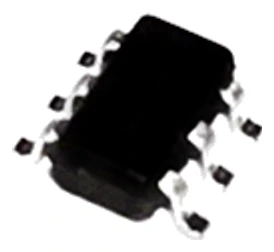
- SOT-23-6
- Configuration
- N+N
- VDS_Max
- 20 V
- ID
- 6 A
- VGS(th)_Typ
- 0.85 V
- Vth Min
- 0.55 V
- Vth Max
- 1.15 V
- RDS(ON)_Typ @VGS=4.5V
- 20 mΩ
- RDS(ON)_Max @VGS=4.5V
- 25 mΩ
- VGS_Max
- ±10 V
- Tj
- -55~+150 °C
- Ciss_Typ
- 370 pF
- Coss_Typ
- 89 pF
- Crss_Typ
- 10 pF
- Qg_Typ
- 7.5 nC
- RDS(ON)_Typ @VGS=2.5V
- 27 mΩ
- RDS(ON)_Max @VGS=2.5V
- 35 mΩ
Not sure how to choose? Read the LV & MV MOSFETs Selection Guide →
Online Datasheet
Full text of the synapsechip.com datasheet; refer to the latest revision for updates.

SYN8205A
20V Dual N-Channel Enhancement Mode MOSFET
DATASHEET
Features
- High Power and Current Handling Capability
- Lead-Free Product
- Surface-Mount SOT-23-6 Package
Applications
- Battery Protection
- Battery-Powered Systems
- Power Management in Notebook Computers
- Portable Equipment
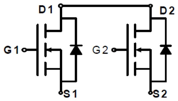
Pin Configuration
| Terminal | Description |
|---|---|
| G1 / G2 | Gate of MOSFET 1 / MOSFET 2 |
| S1 / S2 | Source of MOSFET 1 / MOSFET 2 |
| D1 · D2 | Common drain (internally connected) |
Two N-channel enhancement-mode MOSFETs in a common-drain (back-to-back) configuration for single-cell battery charge / discharge protection.
Absolute Maximum Ratings (1)
(@ TA = 25 °C)
| Parameter | Symbol | Maximum | Units |
|---|---|---|---|
| Drain to Source Voltage | VDSS | 20 | V |
| Gate to Source Voltage | VGSS | ±10 | V |
| Drain Current — Continuous | ID | 6 | A |
| Drain Current — Pulsed | IDM | 24 | A |
| Maximum Power Dissipation | PD | 1.05 | W |
| Operating Junction and Storage Temperature Range | TJ, TSTG | −55 to +150 | °C |
| Lead Temperature for Soldering (1/8″ from case, 10 s) | TL | 260 | °C |
Electrical Characteristics (2)
(@ TA = 25 °C, unless otherwise specified.)
Off Characteristics
| Parameter | Symbol | Test Conditions | Min. | Typ. | Max. | Units |
|---|---|---|---|---|---|---|
| Drain to Source Breakdown Voltage | V(BR)DSS | ID = 250 μA, VGS = 0 V | 20 | — | — | V |
| Zero-Gate Voltage Drain Current | IDSS | VDS = 20 V, VGS = 0 V | — | — | 1 | μA |
| Gate-Body Leakage Current | IGSS | VGS = ±12 V, VDS = 0 V | — | — | ±100 | nA |
On Characteristics
| Parameter | Symbol | Test Conditions | Min. | Typ. | Max. | Units |
|---|---|---|---|---|---|---|
| Gate Threshold Voltage | VGS(th) | VDS = VGS, IDS = 250 μA | 0.55 | 0.85 | 1.15 | V |
| Drain to Source On-State Resistance | RDS(on) | ID = 3 A, VGS = 4.5 V | — | 20 | 25 | mΩ |
| Drain to Source On-State Resistance | RDS(on) | ID = 3 A, VGS = 3.8 V | — | 24 | 26 | mΩ |
| Drain to Source On-State Resistance | RDS(on) | ID = 2 A, VGS = 2.5 V | — | 27 | 35 | mΩ |
Dynamic Characteristics
| Parameter | Symbol | Test Conditions | Min. | Typ. | Max. | Units |
|---|---|---|---|---|---|---|
| Input Capacitance | Ciss | VGS = 0 V, VDS = 10 V, f = 1 MHz | — | 370 | — | pF |
| Output Capacitance | Coss | VGS = 0 V, VDS = 10 V, f = 1 MHz | — | 89 | — | pF |
| Reverse Transfer Capacitance | Crss | VGS = 0 V, VDS = 10 V, f = 1 MHz | — | 10 | — | pF |
| Turn-On Delay Time | td(on) | VDD = 10 V, ID = 3 A, VGS = 4.5 V, RGEN = 10 Ω | — | 200 | — | ns |
| Turn-On Rise Time | tr | VDD = 10 V, ID = 3 A, VGS = 4.5 V, RGEN = 10 Ω | — | 236 | — | ns |
| Turn-Off Delay Time | td(off) | VDD = 10 V, ID = 3 A, VGS = 4.5 V, RGEN = 10 Ω | — | 36 | — | ns |
| Fall Time | tf | VDD = 10 V, ID = 3 A, VGS = 4.5 V, RGEN = 10 Ω | — | 165 | — | ns |
Gate Charge Characteristics
(Test Conditions: VDS = 10 V, VGS = 4.5 V, ID = 1 A.)
| Parameter | Symbol | Min. | Typ. | Max. | Units |
|---|---|---|---|---|---|
| Total Gate Charge | Qg | — | 7.5 | — | nC |
| Gate-Source Charge | Qgs | — | 3.0 | — | nC |
| Gate-Drain Charge | Qgd | — | 1.5 | — | nC |
Body Diode Characteristics
| Parameter | Symbol | Test Conditions | Min. | Typ. | Max. | Units |
|---|---|---|---|---|---|---|
| Diode Forward Voltage | VSD | IS = 2.8 A, VGS = 0 V | — | 0.7 | 1.3 | V |
Notes
- Stresses exceeding those listed in the Absolute Maximum Ratings may damage the device; functional operation beyond those limits is not implied and reliability may be affected.
- Product parametric performance is indicated in the Electrical Characteristics for the listed test conditions; performance under other conditions is not implied.
Important Notice
Information in this document is provided in connection with 突触半导体 products and is subject to change without notice. Customers are responsible for verifying that the product is suitable for their application; no license to any intellectual property right is granted by this document.
SYN8205A · Rev 1.0 · 2026-07 深圳市突触半导体有限公司 · synapsechip.com Page 1–2 of 2