
NFC and RFID are often lumped together as one "contactless identification" category to be compared on a parameter table, but what actually shapes the direction of a design is the frequency band. The band isn't just an RF parameter — it ties into an entirely different reader ecosystem and protocol family. Pick the wrong band, and what needs replacing isn't one chip, but the whole reading infrastructure.
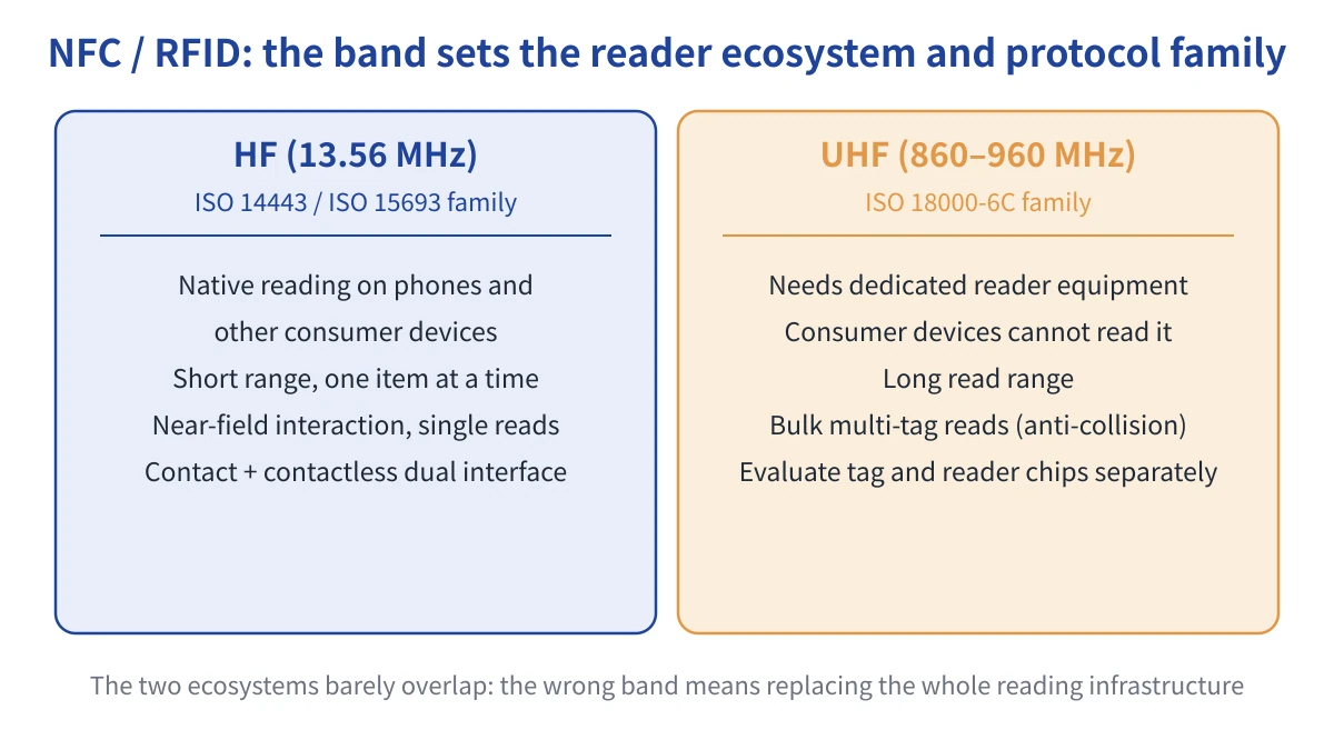
The HF and UHF routes: protocol families, reading devices and typical use
The Band Sets the Ecosystem Position Before Any Part Number Does
Operating in the tens-of-MHz high-frequency band means running on a protocol family built around ISO14443 and ISO15693. Its ecosystem value is that consumer devices such as smartphones generally have native reading capability built in, so no dedicated equipment is needed — but read range is short and identification happens one item at a time, making it a fit for near-field interaction and single-item reads. Operating in the hundreds-of-MHz ultra-high-frequency band means running on a protocol family built around ISO18000-6C: longer read range and the ability to identify multiple tags in bulk, but it depends on dedicated reader equipment, since consumer devices generally can't read it directly. The downstream hardware ecosystems for these two routes barely overlap, so before a design is locked in, the question has to be asked first: is the reading side a consumer's phone, or dedicated equipment the enterprise owns?
Interface Form Factor Sets How Much Room the Back-End Process Has
Building both a contact and a contactless interface into a single chip is common in cards and wearable form factors that need both reading methods to coexist, and the hard part usually isn't protocol compatibility — it's the freedom left for the packaging process once the chip is locked in. How the antenna mates with the module, and how the embedding process interacts with the carrier material, both have to be locked in step with the chip choice, and rework costs run higher than for a single contactless tag; the security mechanism tier for authentication or payment-grade applications needs to be settled early too, since it's very hard to add once the design is finalized. Tag chips and reader chips follow the same two-logic split: for a tag chip, what matters is low power draw and impedance matching with the antenna, with actual read range a joint outcome of the two; for a reader chip, what matters is whether the protocol stack covers the multi-tag anti-collision process, which directly affects identification throughput in dense-tag scenarios — and keeping pin compatibility across generations spares a re-validation cycle.
Making the Call, and Where Teams Trip Up
Start by determining whether the reading side is a consumer device or dedicated equipment, which settles the band; in the high-frequency case, decide whether dual-interface coexistence is actually needed; in the ultra-high-frequency case, evaluate tag chips and reader chips separately. Common pitfalls: treating a lab-measured read range as a field-representative number while ignoring antenna design and mounting environment; locking in the package form too late, forcing the manufacturing process chain to be rebuilt; and leaving security-certification requirements unsettled early on, when they can no longer be fixed once the design is finalized. Once the band and interface form are settled, the on-site selection tool compares by certification and package; antenna matching and security-tier trade-offs are assessed together with our engineers.