
Choosing a PD protocol chip often gets reduced to "does it support PD," but what actually determines the charging experience comes down to two axes: how broadly the protocol stack covers device ecosystems, and whether protocol negotiation and power conversion are kept separate or integrated. The first determines whether a connected device gets the power it's entitled to; the second determines where the design lands on BOM count, board area and thermal budget.
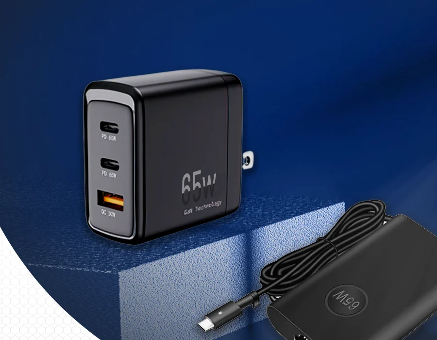
PD fast-charge application key visual. Image: HYASIC
PD itself is a continuously evolving protocol family: beyond the base handshake, it now includes programmable power extensions for a wider voltage range. On the device side, though, many products still layer vendor-defined proprietary handshake mechanisms on top. A protocol chip that only implements the base handshake falls back to the lowest charging rate whenever it meets a device running a proprietary protocol. That is a common root cause behind "rated power never delivered" complaints — usually a failed negotiation, not a power-stage fault. Selection should also confirm whether the protocol stack is a fixed state machine or can be extended through firmware updates — otherwise a minor protocol revision forces a wholesale part-number change.
On integration, keeping the protocol controller and power stage separate offers more flexibility: the same protocol chip can be reused across different power platforms. The costs are one extra component and extra board area for routing and heat. There is also a dynamic-response requirement: when the protocol commands a power step, the power stage must keep pace; if it lags, overshoot or false under-voltage trips can follow — and these issues typically only surface in system-level co-testing. A combined protocol-plus-buck solution folds negotiation and power conversion into one chip. Component count and board area shrink noticeably, which suits products with a fixed power tier and tight space — but the power range is locked by that chip's own input/output window, so a product line spanning multiple power tiers needs multiple part numbers. The same logic applies on the AC/DC side: an external power switch preserves the freedom to choose the switch, while an integrated switch saves a discrete component but has its power ceiling framed in advance by the built-in switch's conduction characteristics. Across the product lines we distribute, PD protocol chips, combined protocol-plus-buck solutions, and both AC/DC routes — external-switch controllers and integrated-switch parts — are all covered.
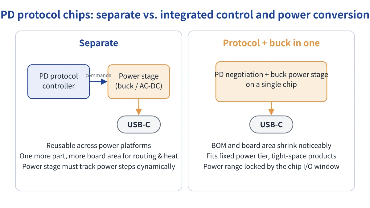
Protocol control and power conversion: separate versus protocol-plus-buck integration
For engineering teams, the more useful starting point isn't the parameter table. Clarify first how wide a device ecosystem the product must cover, and whether the power platform is a single fixed tier or spans multiple tiers — then decide the trade-off between protocol coverage and integration approach. Once the power tier and target device ecosystem are settled, the on-site selection tool can narrow candidates by power and package; questions about protocol compatibility go to our engineers.