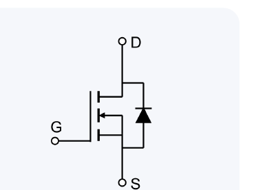
产品详情
SYN8205W
突触半导体旗下产品
参数规格
- 结构
- N+N
- 漏源电压 VDS
- 20 V
- 阈值电压 VGS(th) 典型
- 0.6 V
- Die Size (μm×μm)
- 741*800(含划片槽)
- Gross Die (8" wafer)
- 100000
- Wafer Thickness (μm)
- 150±15
- 栅源电压 VGS 最大
- ±12 V
- 导通电阻 RDS(ON)@4.5V 典型
- 21 mΩ
- 导通电阻 RDS(ON)@4.5V 最大
- 25 mΩ
- 导通电阻 RDS(ON)@2.5V 典型
- 26 mΩ
- 导通电阻 RDS(ON)@2.5V 最大
- 30 mΩ
- 结温 Tj
- -55~+150 °C
不确定怎么选?阅读《MOSFET 晶圆/裸片选型指南》 →
在线规格书
以下为突触半导体规格书全文,如有更新以最新版本为准。

SYN8205W
20V Dual N-Channel Enhancement Mode MOSFET
WAFER DATASHEET
Features
- Power MOSFET
- Low Gate Charge
- Excellent RDS(ON)
Applications
- Load Switch, Motor Driving
- DC-DC Converters
- Power Management Functions
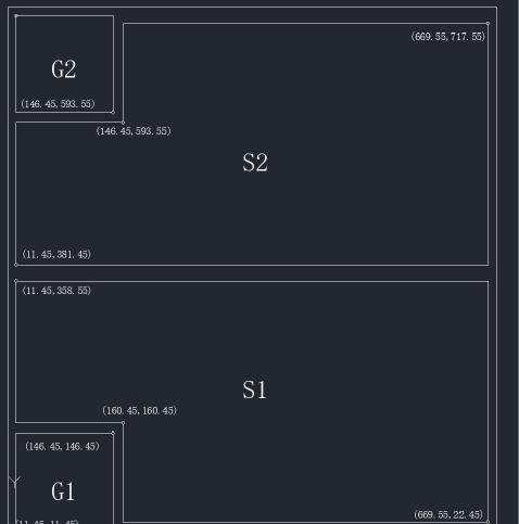
Chip Information
| Parameter | Value |
|---|---|
| Die Size (include scribe line) | 741 μm × 800 μm |
| Gate Pad Size | 135 μm × 135 μm |
| Source Pad Size | Full Opening Area |
| Scribe Line Size | 60 μm |
| Wafer Thickness | 150 μm ± 15 μm |
| Wafer Diameter | 200 mm |
| Front Metal Composition & Thickness | AlCu, 4 μm |
| Back Metal Composition & Thickness | Ti-Ni-Ag, 1kÅ-2kÅ-10kÅ |
| Passivation | SRO 6kÅ + SiN 5kÅ |
| Polyimide | NA |
| Gross Die (approximately) | 100,000 (50,000 × 2) |
Maximum Ratings
(@ TA = 25 °C, unless otherwise specified.)
| Characteristic | Symbol | Value | Units |
|---|---|---|---|
| Drain–Source Voltage | VDS | 20 | V |
| Gate–Source Voltage | VGS | ±12 | V |
| Continuous Drain Current | ID | 6 | A |
| Junction Temperature Range | TJ | −55 ~ +150 | °C |
Electrical Characteristics
(@ TA = 25 °C, unless otherwise specified.)
Off Characteristics
| Parameter | Symbol | Test Conditions | Min. | Typ. | Max. | Units |
|---|---|---|---|---|---|---|
| Drain–Source Breakdown Voltage | V(BR)DSS | VGS = 0 V, ID = 250 μA | 20 | — | — | V |
| Zero Gate Voltage Drain Current | IDSS | VDS = 20 V, VGS = 0 V, TJ = 25 °C | — | — | 1.0 | μA |
| Gate–Body Leakage Current | IGSS | VGS = ±12 V, VDS = 0 V | — | — | ±100 | nA |
On Characteristics (1)
| Parameter | Symbol | Test Conditions | Min. | Typ. | Max. | Units |
|---|---|---|---|---|---|---|
| Gate Threshold Voltage | VGS(th) | VGS = VDS, ID = 250 μA | 0.4 | 0.6 | 0.9 | V |
| Static Drain–Source On-Resistance (FT) | RDS(ON) | VGS = 4.5 V, ID = 4 A | — | 21 | 25.0 | mΩ |
| Static Drain–Source On-Resistance (FT) | RDS(ON) | VGS = 2.5 V, ID = 3 A | — | 26 | 30.0 | mΩ |
| Static Drain–Source On-Resistance (CP) | RDS(ON) | VGS = 4.5 V, ID = 1 A | — | — | 25.0 | mΩ |
| Static Drain–Source On-Resistance (CP) | RDS(ON) | VGS = 2.5 V, ID = 1 A | — | — | 30.0 | mΩ |
| Diode Forward Voltage | VSD | IS = 2.0 A, VGS = 0 V | — | 0.7 | 1.0 | V |
说明:FT = Final Test(成品测试),CP = Chip Probe(中测/晶圆测试);两组 RDS(ON) 分别对应封装成品测试条件与晶圆探针测试条件,原文如此并列,转写未合并。
Notes
- Measured under pulsed conditions. Pulse width ≤ 300 μs, duty cycle ≤ 2%.
- RDS(ON) value is referred by the device assembled in SOT26.
Important Notice
Information in this document is provided in connection with 突触半导体 products and is subject to change without notice. Customers are responsible for verifying that the product is suitable for their application; no license to any intellectual property right is granted by this document.
SYN8205W · Rev 1.1 · 2026-08 深圳市突触半导体有限公司 · synapsechip.com Page 1 of 1