Home / Products / LV & MV MOSFETs / SMT6003CLS Specifications
Package TO220-3L
Configuration N
VDS_Max 60 V
ID 171 A
RDS(ON)_Max @VGS=10V 3.4 mΩ
Automotive (Y/N) N
VGS(th)_Typ 1.7 V
RDS(ON)_Typ @VGS=10V 2.8 mΩ
RDS(ON)_Typ @VGS=4.5V 3.5 mΩ
RDS(ON)_Max @VGS=4.5V 4.2 mΩ
VGS_Max ±20 V
Tj 175 °C
EAS_Max 436 mJ
Ciss_Typ 2816 pF
Coss_Typ 1326 pF
Crss_Typ 77 pF
Qg_Typ 53 nC
ESD No
MPQ 1000 pcs
MOQ 5000 pcs
App: Motor Drive Y
App: Battery Protection Y
App: General Switch Y Not sure how to choose? Read the LV & MV MOSFETs Selection Guide →
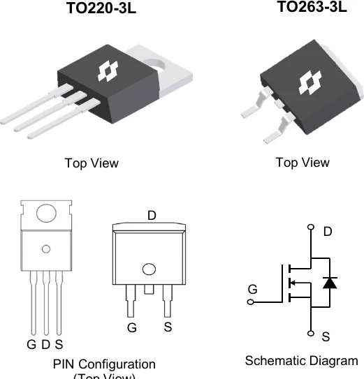
Package & Schematic Package outline · Pin configuration · Schematic (from SineSemi official datasheet) Online Datasheet Compiled from the manufacturer's datasheet; the official document prevails.
SMT6003CLS
60V N-Channel Power MOSFET
Product Summary
VDS
RDS (ON), max
ID , max
— V
— mΩ @ VGS = 10V
171 A
TO220-3L
Maximum Ratings (@ TA = 25°C, unless otherwise specified.)
Parameter
Symbol
Value
Units
Drain - Source Voltage
VDS
60
V
Gate - Source Voltage
VGS
±20
V
Continuous Drain Current (VGS = 10V) (1)
ID @ TC = 25°C
171
A
ID @ TC = 100°C
121
A
Pulsed Drain Current (2)
IDM
682
A
Single Pulse Avalanche Energy (3)
EAS
436
mJ
Single Pulse Avalanche Current (L = 0.1mH)
IAS
50
A
Power Dissipation
PD @ TC = 25°C
150
W
PD @ TC = 100°C
75
W
Junction & Storage Temperature Range
TJ , TSTG
-55~+175
°C
Thermal Characteristics
Parameter
Symbol
Typ
Max
Unit
Thermal Resistance, Junction-to-Ambient (4)
R_θJA
36
45
°C/W
Thermal Resistance, Junction-to-Case (5)
R_θJC
0.80
1.0
°C/W
Electrical Characteristics (@ TJ = 25°C, unless otherwise specified.)
Off Characteristics
Parameter
Symbol
Test Condition
Min
Typ
Max
Units
Drain-Source Breakdown Voltage
V(BR)DSS
VGS = 0V, ID = 250µA
60
—
—
V
VDS = 60V, VGS = 0V
—
—
1.0
µA
Zero Gate Voltage Drain Current
IDSS
TJ = 125°C
—
—
100
µA
Gate-Source Leakage Current
IGSS
VGS = ±20V, VDS = 0V
—
—
±100
nA
On Characteristics
Parameter
Symbol
Test Condition
Min
Typ
Max
Units
Gate Threshold Voltage
VGS (th)
VGS = VDS , ID = 250µA
1.2
1.7
2.5
V
Static Drain-Source On-Resistance
RDS (on)
—
—
—
—
mΩ
Forward Transconductance
gfs
VDS = 5.0V, ID = 20A
—
24
—
S
Diodes Forward Voltage
VSD
IS = 2.0A, VGS = 0V
—
0.7
1.2
V
Dynamic Characteristics
Parameter
Symbol
Test Condition
Min
Typ
Max
Units
Input Capacitance
Ciss
—
2816
—
pF
Output Capacitance
Coss
VDS = 30V, VGS = 0V, f = 1MHz
—
1326
—
pF
Reverse Transfer Capacitance
Crss
—
77
—
pF
Gate Resistance
Rg
VGS = 0V, VDS = 0V, f = 1MHz
—
1.4
—
Ω
Switching Characteristics
Parameter
Symbol
Test Condition
Min
Typ
Max
Units
Turn-On Delay Time
td (on)
—
5.0
—
ns
Rise Time
tr
VDS = 30V, VGS = 10V
—
13
—
ns
Turn-Off Delay Time
td (off)
ID = 20A, RGEN = 3.0Ω
—
46
—
ns
Fall Time
tf
—
23
—
ns
Gate Charge Characteristics
Parameter
Symbol
Test Condition
Min
Typ
Max
Units
Total Gate Charge (VGS = 10V)
Qg
—
53
—
nC
Total Gate Charge (VGS = 4.5V)
Qg
—
27
—
nC
Gate-Source Charge
Qgs
VDS = 30V, ID = 20A
—
7.8
—
nC
Gate-Drain Charge
Qgd
—
12
—
nC
Gate Plateau Voltage
Vplateau
—
2.9
—
V
Drain-Source Diode Characteristics
Parameter
Symbol
Test Condition
Min
Typ
Max
Units
Body Diode Reverse Recovery Time
trr
IS = 20A, di/dt = 100A/µs
—
47
—
ns
Body Diode Reverse Recovery Charge
Qrr
TJ = 25°C
—
42
—
nC
Diode Forward Current
IS
TJ = 25°C
—
—
125
A
Notes:
This current is chip limited, which is calculated based on Rthjc. 2. This current is calculated on single pulse with 10μs Single Pulse. 3. Defined by design, not subject to production test, EAS condition: TJ=25°C, VDD=30V, VGS=10V, L=1.0mH. 4. Device mounted on FR-4 substrate PC board with 2oz copper in 1inch square cooling area. 5. Thermal resistance from junction to the exposed pad. 6. Short duration pulse test used to minimize self-heating effect. 7. Defined by design, not subject to production.